Overview
Darsena is no longer being manufactured, and we're in the process of defining a next generation maker board for Private Island.
The next generation system will abandon the Ardunio format and strive for lower cost, better signal integrity, and greater flexibility.
Darsena™ is an FPGA-based, dual Gigabit Ethernet, Arduino form-factor development board for the open source Private Island project. Private Island ® is an open source FPGA stack targeting network security, privacy, IoT, test & measurement, and control applications.
This document currently applies to our v0.2 boards (figure below shows v0.1).
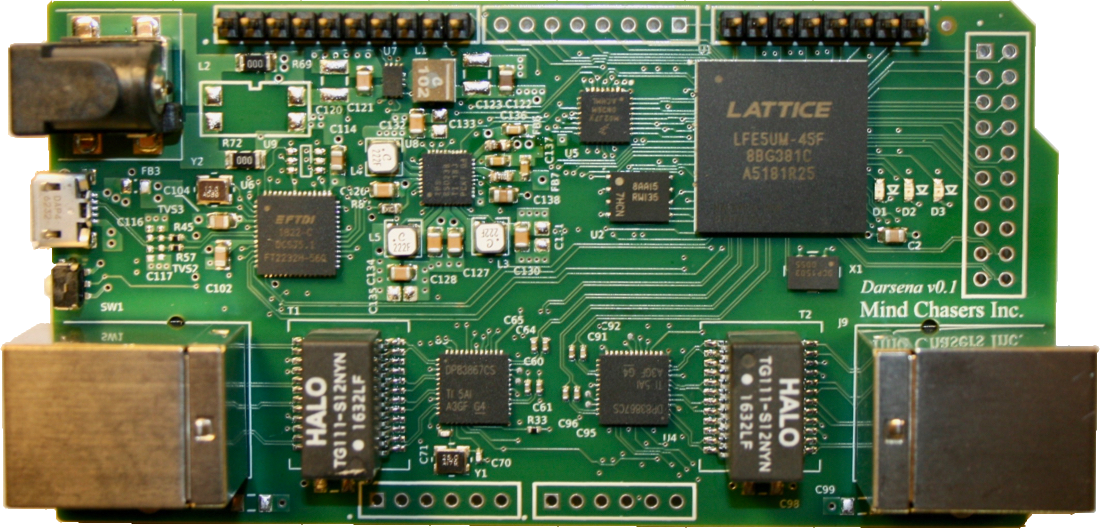
Figure 2 below shows a system block diagram of the Darsena board. A Lattice ECP5UM FPGA controls and processes Ethernet traffic for two Texas Instruments DP83867 Gigabit Ethernet PHYs. An NXP K02 ARMv7-based microcontroller (µC) is provided for receiving and transmitting packets via the FPGA. Dual integrated debug is enabled via an FTDI FT2232H device that is capable of simulataneous debug of both the FPGA and µC.
Arduino-compatible expansion connectors are available and some pins have been re-defined to carry high-speed data to and from the FPGA for port expansion (e.g., third Ethernet port).
The board is powered from a a single external DC supply (5V to 12V). Multiple on-board buck regulators and LDOs provide the necessary voltage rails to power the on-board devices and shields.
The nominal power draw for a stand alone Darsena with both Gigabit PHYs fully operational is approximately 3 W.
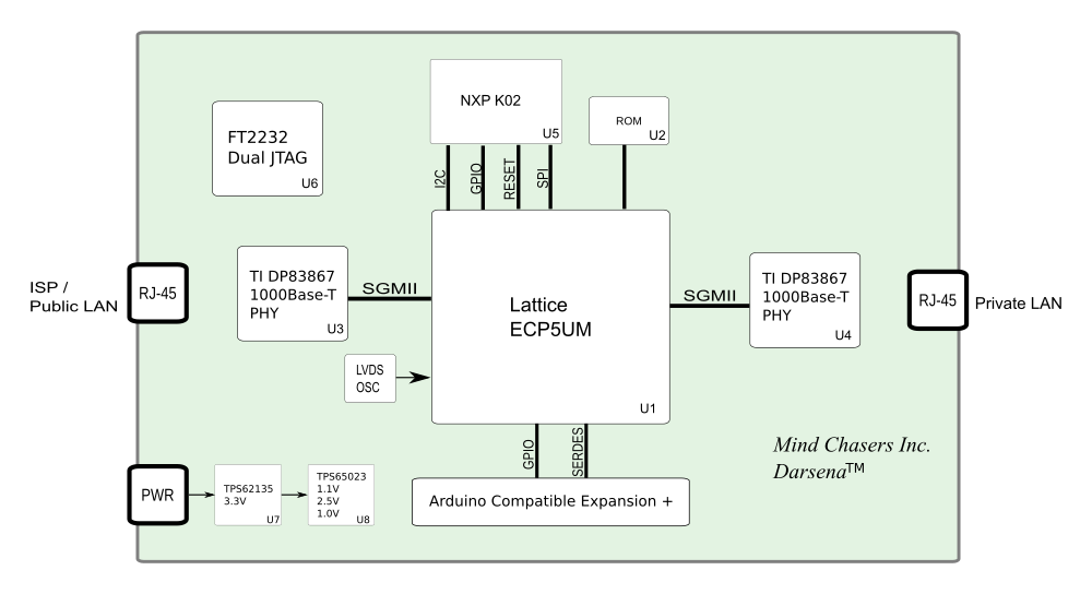
Table of Contents:
- Lattice ECP5UM FPGA
- Texas Instruments DP83867 PHY
- NXP Kinetis K02 µC
- Arduino Compatibility
- Power
- Reset
- FTDI FT2232H Integrated Debug
Lattice ECP5UM FPGA
Lattice ECP5UM Overview
- 45K LUT FPGA in a 381 ball BGA package
- Integrated 4-channel PCS/SERDES for interfacing to PHYs and expansion. An external LVDS reference clock drives the PCS circuitry.
- 1944 kbit of dedicated embedded memory and multiple signal processing engines
- Supported by the Lattice Diamond IDE that includes a virtual logic analyzer (Reveal) for triggering on user definable events including complex network packet classification.
- For further ECP5 information, please see this summary of the ECP5 for Private Island
- Micron SPI ROM for FPGA boot. ROM can be programmed via Lattice Diamond / JTAG.
- Voltages: 1.1V, 1.1VA, 2.5V, 2.5VA, 3.3V
FPGA Configuration
Darsena provides a 128 Mbit discrete SPI ROM for external programming. The FPGA is configured for Master SPI mode and loads the ROM upon power up. Additional notes are provided below:
- Each worst case ECP5UM-45 image with EBRs initialized requires less than 16Mb
- The ECP5UM has an internal POR circuit and holds all user I/O output buffers in tri-state during configuration (offline) mode. During this time, the input buffers are pulled low with a weak internal pull-down.
- The µC can restart a configuration cycle by asserting FCFG_PGMN.
- The µC can determine the status of a configuration cycle by polling the FCFG_DONE signal. Note that this is a bidirectional, open drain signal, and the µC should not drive this signal unless it wishes to hold off the completion of a configuration cycle. Also note that the FCFG_DONE signal is not meaningful during a JTAG programming cycle.
- Maximum MCLK frequency supported is 62 MHz.
Configuration ROM
- Micron MT25QL128ABA1EW7-0SIT:
- 25Q: SPI NOR
- L: 3.3V
- 128: 128Mb
- A: 1 die
- BA: 2nd Gen, Die Rev A
- 1: HOLD# Pin
- E: 64KB sectors, 4KB and 32KB sub-sectors
- W7: 8-pin W-PDFN, 6 x 5mm
Texas Instruments DP83867 PHY
DP83867 Overview
- Gigabit Ethernet Phy
- MAC Interfaces: RGMII / SGMII (SGMII is utilized on Darsena)
- Excellent EE Forum
- Low latency for both 100Mbps and 1Gbps modes, < 400ns Start of Frame Detect for IEEE 1588 time stamp
- Path latencies: TX < 90 ns, RX < 290 ns
- Extensive built in diagnostic capabilities
- Voltages: 1.0V, 2.5V, and 3.3V
MDIO
- FPGA drives MDIO bus for both PHYs via separate decdicated buses. This enables both buses to be used in parallel.
- MDC frequency (f) = 9.7 MHz
- MDC period (T): 0.103 µs
NXP Kinetis K02 µC
K02 Overview
- 100 MHz ARM Cortex-M4 core
- 128 KB of embedded flash and 16 KB of RAM
- I2C for FPGA controller interface, SPI for memory interface
- ADC / DAC support
- Full featured MCUXpresso SDK
- Supported by GNU Arm Embedded Toolchain
- Excellent Pin / Clock configuration tool
- NXP Community Forum
- Developers can choose to use NXP's MCUXpresso or mainline Eclipse for an IDE
SPI Interface
- K02 is SPI master, FPGA is the slave.
- 8-bit transfers are utilized and described further in the External Register and Memory Interface document.
- CPOL=0, CHPA=0
- No external pullups required since interface is point-to-point. However, utilize internal pullup on SPI_PCSN.
I2C Interface
- K02 is I2C master. FPGA and PMIC are slaves
- PMIC's device address is 0x48
- FPGA's device address is 0x10
K02 Interrupts
- K02 NMI Interrupt is driven by the PMIC interrupt (PMIC_INTN) and has an external pullup.
- PHYs interrupt FPGA and in turn interrupt K02
UART
- Routed through the FPGA and potentially onto an Ardunio expansion connector for use by an external UART circuit.
Arduino Compatibility
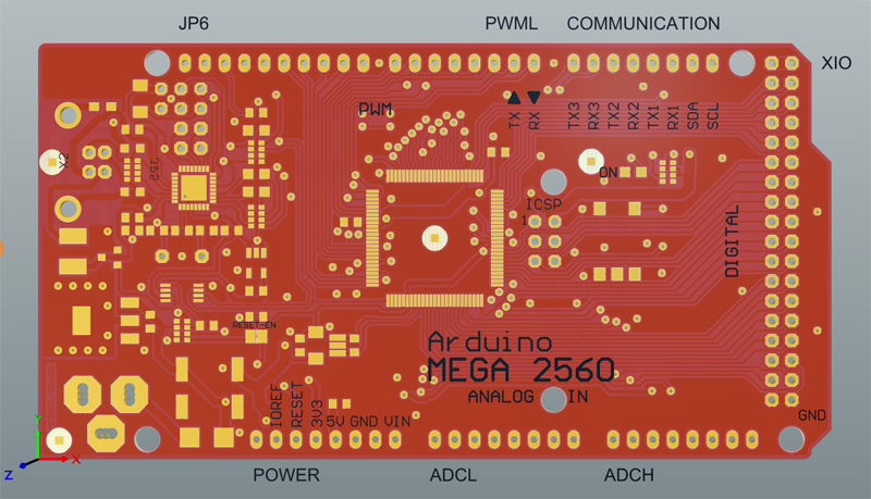
Darsena is the same form factor as the Arduino MEGA 2560 and supports a subset of the MEGA pins. The figure below shows a 3D rendering of the MEGA PCB based on the download available on the Arduino web site. The tables below review the compatibility of the pinout starting in the upper left with connector JP6 and moving clockwise to POWER. Note, the connector names are shown in the figure on the outside of the PCB and are positioned near pin 1.
Note that this documentation is for pre-released versions of Darsena. All pins are under review and subject to change.
JP6 Connector
JP6 is a 10-pin connector numbered left-to-right in the upper left of the board. For Darsena, the µC and FPGA JTAG signals are routed to JP6 to enable the use of an external debugger or to re-provision the use of the I/O from the FTDI FT2232H. When using an external debugger, the FTDI I/O must be tri-stated via programming from the USB bus.
| Pin | Arduino | Darsena | Notes |
|---|---|---|---|
| 1 | SCL | FPGA_TCK | |
| 2 | SDA | FPGA_TDI | |
| 3 | AREF | N/C | no connect |
| 4 | GND | GND | |
| 5 | PB7 | FPGA_TDO | |
| 6 | PB6 | FPGA_TMS | |
| 7 | PB5 | MICRO_TMS | |
| 8 | PB4 | MICRO_TDO | |
| 9 | PH6 | MICRO_TDI | |
| 10 | PH5 | MICRO_TCK |
PWML Connector
PWML is an 8-pin connector numbered right-to-left in the upper middle of the board. All of these signals map to FPGA I/O, and the ECP5 pin name is provided in the table below. In some instances, the pin may also have an alternate function. This is called out in the notes column below.
| Pin | Arduino | Darsena | Notes |
|---|---|---|---|
| 1 | PE0 | PL11B | ULC_GPLL0C |
| 2 | PE1 | PL11C | |
| 3 | PE4 | PL11A | ULC_GPLL0T |
| 4 | PE5 | PL14B | |
| 5 | PG5 | PL14C | |
| 6 | PE3 | PL14D | |
| 7 | PH3 | PL23A | |
| 8 | PH4 | PL23C | VREF |
COMMUNICATION
COMMUNICATION is an 8-pin connector numbered right-to-left in the upper right corner of the board. All of these signals map to FPGA I/O, and the ECP5 pin name is provided in the table below.
| Pin | Arduino | Darsena | Notes |
|---|---|---|---|
| 1 | SCL | PT85B | URC_GPLL1C |
| 2 | SDA | PT85A | URC_GPLL1T |
| 3 | RXD1 | PT83A | |
| 4 | TXD1 | PT80A | |
| 5 | RXD2 | PT56A | |
| 6 | TXD2 | PT36A | PCLKT0 |
| 7 | RXD3 | PT18A | |
| 8 | TXD3 | PT4A |
XIO
The Arduino MEGA XIO connector is a dual row connector, 2x18. It provides many additional I/O for expansion. Darsena provides a 2x10 connector offset by one row (doesn't support the top pair of 5V pins). The first 14 pins support general purpose I/O (GPIO), and the last 4 pins support two pairs of LVDS for expansion of a third Ethernet PHY. The Ethernet feature should be considered experimental for now.
ADCH
Darsena does not support the ADCH connector.
ADCL
Arduino utilizes this 8-pin connector for analog inputs (ADC0 through ADC7 from left to right). Some of the K02's analog functionality is routed to these pins. See the table below for details.
| Pin | Arduino | Darsena | Notes |
|---|---|---|---|
| 1 | ADC0 | N/C | |
| 2 | ADC1 | N/C | |
| 3 | ADC2 | GND | |
| 4 | ADC3 | K02 DAC0 | |
| 5 | ADC4 | K02 ADC0_DM | Can be used as single ended |
| 6 | ADC5 | K02 ADC0_DP | Can be used as single ended |
| 7 | NO PIN | ||
| 8 | ADC7 | NO PIN |
POWER
Arduino utilizes this 8-pin connector for power and reset. The pin ordering is left to right. Darsena does not currently support 5V power on the expansion connectors, but this is under investigation.
| Pin | Arduino | Darsena | Notes |
|---|---|---|---|
| 1 | N/C | NO PIN | |
| 2 | 5V | NO PIN | |
| 3 | RESET | N/C | |
| 4 | 3.3V | 3.3V | |
| 5 | 5V | N/C | |
| 6 | GND | GND | |
| 7 | GND | GND | |
| 8 | VIN | N/C |
Power Circuitry
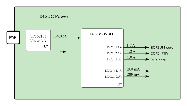
Darsena requires an external DC power source connected to its barrel connector. The voltage must be between 5V and 12V. Stand alone operation can be as low as 3W but may increase substantially depending on FPGA and / or shield utilization.
The wall supply is converted to 3.3V by a TI TPS62135 buck regulator.
The TI TPS65023B PMIC provides three step down buck regulators and two LDOs:
- 1.1V, 1.7 A
- 2.5V, 1.2 A
- 1.0V, 1 A
- LDO1: 1.1V, 200 mA
- LDO2: 2.5V, 200 mA
The three buck regulators are enabled by default due to a pull up resistor tied to the DCDC enable pins. The regulators provide the required voltage levels using fixed resistor dividers on the DEFDCDC pins. The K02 can subsequently disable all bucks by driving the enable (PMIC_DCDC_E) low or individually via the PMIC's I2C interface.
The two LDO regulators are disabled by default due to an external pull down resistor (R35). This is required since their default voltage rails are not what is needed and sequencing is required for these rails. The K02 is required to progam the LDOs adequately before enabling the LDO in sequence (see FPGA power sequencing below).
TI TPS65023B notes:
The TPS65023x incorporates three synchronous step-down converters operating typically at 2.25-MHz, fixed frequency pulse width modulation (PWM) at moderate to heavy-load currents. At light-load currents, the converters automatically enter the power save mode (PSM), and operate with pulse frequency modulation (PFM). The VDCDC1 converter, which powers the ECP5 core at 1.1V, is capable of delivering 1.7-A output current, the VDCDC2 converter is capable of delivering 1.2 A and the VDCDC3 converter, which powers the PHY cores at 1.0V, is capable of delivering up to 1 A.
The core voltage (DCDC1) can be reprogrammed through the serial interface in the range of 0.8 V to 1.6 V with a programmable slew rate. The converter is forced into PWM operation whilst any programmed voltage change is underway, whether the voltage is being increased or decreased. The DEFCORE and DEFSLEW registers are used to program the output voltage and slew rate during voltage transitions.
The PMIC DCDCs can be synchronized out of phase from one another, reducing the peak noise at the switching frequency.
FPGA power sequencing notes from Lattice ECP5 datasheet:
- "It is recommended that the I/O buffers be powered-up prior to the FPGA core fabric. VCCIO supplies should be powered-up before or together with the VCC and VCCAUX supplies." (Page 40 of DS)
- "If the ECP5/ECP5-5G device is using Master SPI mode to download configuration data from external SPI Flash, it is required to ramp VCCIO8 above VIH of the external SPI Flash, before at least one of the other two supplies (VCC and/or VCCAUX) is ramped to VPORUP voltage level" (Page 49 of DS)
- "For LFE5UM/LFE5UM5G devices, it is required to power up VCCA, before VCCAUXA is powered up." (Page 49 of DS)
- "VCCAUX ramp rate must not exceed 30 mV/us during power-up when transitioning between 0 V and 3 V." (Page 48, Note 4 of DS)

Reset and Boot
The default operation is that both the µC and FPGA boot independently upon powerup, and the µC can subsequently re-trigger an FPGA configuration. The PHYs remain in reset until the µC programmatically releases them via the FPGA.
The FTDI device powers up independently. The FT2232H default configuration on its two ports is RS-232, and a host via USB must re-configure the ports to JTAG / MPSEEE for proper use (e.g., OpenOCD JTAG controller).
Reset Signals:
| Signal | Notes |
|---|---|
| UC_RESETN | Drives K02 Reset Signal. Signal is pulled up with R68. Can be driven low by SW1, FTDI I/O, and 3.3 Buck (U7) PG signal |
| PHY0_RESETN | Drives PHY0 Reset Signal from FPGA. Signal is pulled down with R24. |
| PHY1_RESETN | Drives PHY1 Reset Signal from FPGA. Signal is pulled down with R14. |
| FPGA_RESETN | µC asserts this to reset FPGA after configuration is done. There is no external pull-up or pull-down resistor. FPGA should be programmed with an internal pull-up. |
| FTDI_RESETN | R43 pulls the signal high. |
Reset Sequence:
- External power supply rises above 5V.
- TPS62135 Power Good (PG) signal assertion negates K02 reset
- ECP5 boots based on voltage rail requirements being met
- Under software control, K02 asserts PMIC power enables for LDOs
- K02 releases PHY resets and enables / powers up the FPGA's PCS/SERDES block via I2C controller commands
Additional Reset Notes
- There is a momentary mechanical switch on the edge of Darsena that can assert the K02 reset.
- The active, integrated K02 reset filter should be utilized, and an optional LPF RC filter is provided on the PCB.
- TPS62135 PG is open drain. When low this asserts the K02 RESET_B, which is also open drain. K02 reset will make use of internal filter.
- DP83867CS has an internal POR circuit that asserts regardless of its RESET_N.
- DP83867CS requires a minimum reset pulse width of 1 us.
FTDI FT2232H Integrated Debug
- FTDI FT2232H USB to dual JTAG controller
- Enables debug and programming support of both FPGA and K02
- Enables Reveal virtual logic analyzer
FT2232H Interfaces
Port A is dedicated to K02 JTAG.
Port B either interfaces with ECP5 JTAG or ECP5 UART (TX/RX). The selection depends on the 2-bit 74LVCG126 buffer (U10) and the following:
- FTDI Port B - FPGA JTAG: R67 installed and FTDI_ECP5_JTAGE_E is high or tri-state
- FTDI Port B - FPGA UART: R67 installed and FTDI_ECP5_JTAGE_E driven, low or R67 not installed and FTDI_ECP5_JTAGE_E driven / pulled low
- Note that FTDI_ECP5_JTAGE_E is pulled low during programming by the ECP5.
- One mode of operation is to tri-state FTDI_ECP5_JTAGE_E during FPGA reset but drive low during operation to enable FT2232H to UART operation.
- This logic will most likely change for v0.3



Date: May 25, 2019
Author: Nishant Pani
Comment: