
Overview
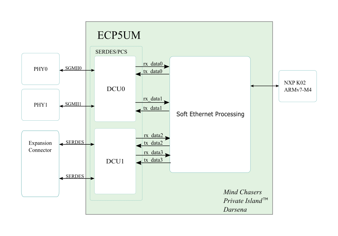
This article describes the usage and configuration of the Lattice ECP5UM SERDES/PCS block for the Private Island ® open source project. The ECP5UM provides two embedded SERDES/PCS channels per Dual-Channel Unit (DCU) and two DCU's per device.
As depicted in the figure below, Private Island utilizes up to four channels for processing via Gigabit PHYs. Two 1000BASE-T PHYs are provided on the Darsena development board with support provided for additional PHYs (e.g., 1000BASE-SX Fiber) via an expansion connector.
This article refers to Lattice's "ECP5 and ECP5-5G SERDES/PCS Usage Guide" TN1261, and it is suggested that the reader have it open while reading this article.
The ECP5UM DCU is a hard macrocell, and it provides a great deal of flexibility for various protocols. For Private Island, the first DCU is configured for 1000-BaseT operation via SGMII PHYs, and the settings are summarized in the table below.
| DCU (PCS/SERDES) Parameter | Setting |
|---|---|
| Protocol | GbE |
| TX/RX serial data rates | 1.25 Gbps |
| TxPLL/CDR PLL Multiplier | 25x |
| REFCLK (DCU0 only)2 | 50 MHz |
| DCU / FPGA data interface width | 8-bit |
| FPGA PCS Clock Rate | 125 MHz |
| Receive CTC | Enabled |
| Receive FIFO | Enabled |
| Transmit FIFO | Enabled |
| Reset Sequence | Disabled2 |
DCU I/O Definition
The Verilog definition for the DCU module is provided in "ecp5um.v", which can be found within the Lattice Diamond installation. For Diamond on Windows 10, the path is <diamond install path>\<release>_x64\synpbase\lib\lucent. In some cases, the module I/O names do not match the signal names provided in the TN1261 documentation. Therefore, a mapping for many of the utilized signals is provided in the tables below.
| DCUA Definition | signal name | I/O | Notes |
|---|---|---|---|
| D_FFC_DUAL_RST | rst_dual_c | I | AUX channel |
| D_FFC_MACRO_RST | serdes_rst_dual_c | I | AUX channel |
| D_FFC_MACROPDB | serdes_pdb | I | AUX channel |
| D_FFC_TRST | tx_serdes_rst_c | I | Only one for both TX channels |
| D_REFCLKI | refclko | I | TX PLL reference clock from EXTREF |
| D_FFS_PLOL | pll_lol | O | Don't use. Use soft logic generated by Clarity instead |
| DCUA Definition | signal name | I/O | Notes |
|---|---|---|---|
| CHX_RX_REFCLK1 | refclko | I | CDR reference clock from EXTREF |
| CHX_FF_RXI_CLK | txi_clk | I | RX FIFO clock from FPGA |
| CHX_FF_TXI_CLK | txi_clk2 | I | TX FIFO clock from FPGA |
| CHX_FF_EBRD_CLK | txi_clk2 | I | CTC FIFO clock from FPGA |
| CHX_FF_TX_D_[0:7] | txdata[0:7] | I | Transmit data bus |
| CHX_FF_TX_D_8 | tx_k | I | Assert for special code-groups |
| CHX_FF_TX_D_10 | xmit | I | Auto negotiation / idle insert |
| CHX_FF_TX_D_11 | tx_disp_correct | I | Assert for DCU to correct disaparity |
| CHX_FFC_SIGNAL_DETECT | signal_detect_c | I | Enable RX link state machine |
| CHX_FFC_LANE_TX_RST | tx_pcs_rst_c | I | Reset TX channel PCS logic |
| CHX_FFC_LANE_RX_RST | rx_pcs_rst_c | I | Reset RX channel PCS logic |
| CHX_FFC_RRST | rx_serdes_rst_c | I | Reset digital logic in SERDES RX channel |
| CHX_FFC_TXPWDNB | tx_pwrup_c | I | TX Channel power up |
| CHX_FFC_RXPWDNB | rx_pwrup_c | I | RX Channel power up |
| CHX_FF_TX_PCLK | tx_pclk | O | Transmit Primary Clock |
| CHX_FF_RX_D_[0:7] | rxdata[0:7] | O | Receive data bus |
| CHX_FF_RX_D_8 | rx_k | O | Asserted for special code-groups |
| CHX_FF_RX_D_9 | rx_disp_err | O | RX disparity error |
| CHX_FF_RX_D_10 | rx_cv_err | O | code violation |
| CHX_FFS_RLOS | rx_los_low_s | O | Loss of signal (LO THRESHOLD RANGE) detection |
| CHX_FFS_LS_SYNC_STATUS | lsm_status_s | O | Channel is synced with commas |
| CHX_FFS_RLOL | rx_cdr_lol_s | O | CDR loss loss of lock |
| CHX_FFS_CC_UNDERRUN() | ctc_urun_s | O | CTC status flag |
| CHX_FFS_CC_OVERRUN() | ctc_orun_s | O | CTC status flag |
| CHX_FFS_SKP_ADDED | ctc_ins_s | O | CTC status flag |
| CHX_FFS_SKP_DELETED | ctc_del_s | O | CTC status flag |
SERDES Client Interface
This interface supports both an alternative method to static configuration of the DCU block as well as some dynamic configuration.
| DCUA Definition | signal name | I/O | Notes |
|---|---|---|---|
| D_SCIWDATA[0:7] | sci_wrdata[0:7] | I | |
| D_SCIADDR[0:5] | sci_addr[0:5] | I | |
| D_SCIENAUX | sci_en_dual | I | Not defined in TN1261 |
| D_SCISELAUX | sci_sel_dual | I | |
| D_SCIRD | sci_rd | I | |
| D_SCIWSTN | sci_wrn | I | |
| D_SCIRDATA[0:7] | sci_rddata[0:7] | O | |
| D_SCIINT | sci_int | O |
| DCUA Definition | signal name | I/O | Notes |
|---|---|---|---|
| CHX_SCIEN | sci_en | I | Not defined in TN1261 |
| CHX_SCISEL | sci_sel | I |
DCU Clocking
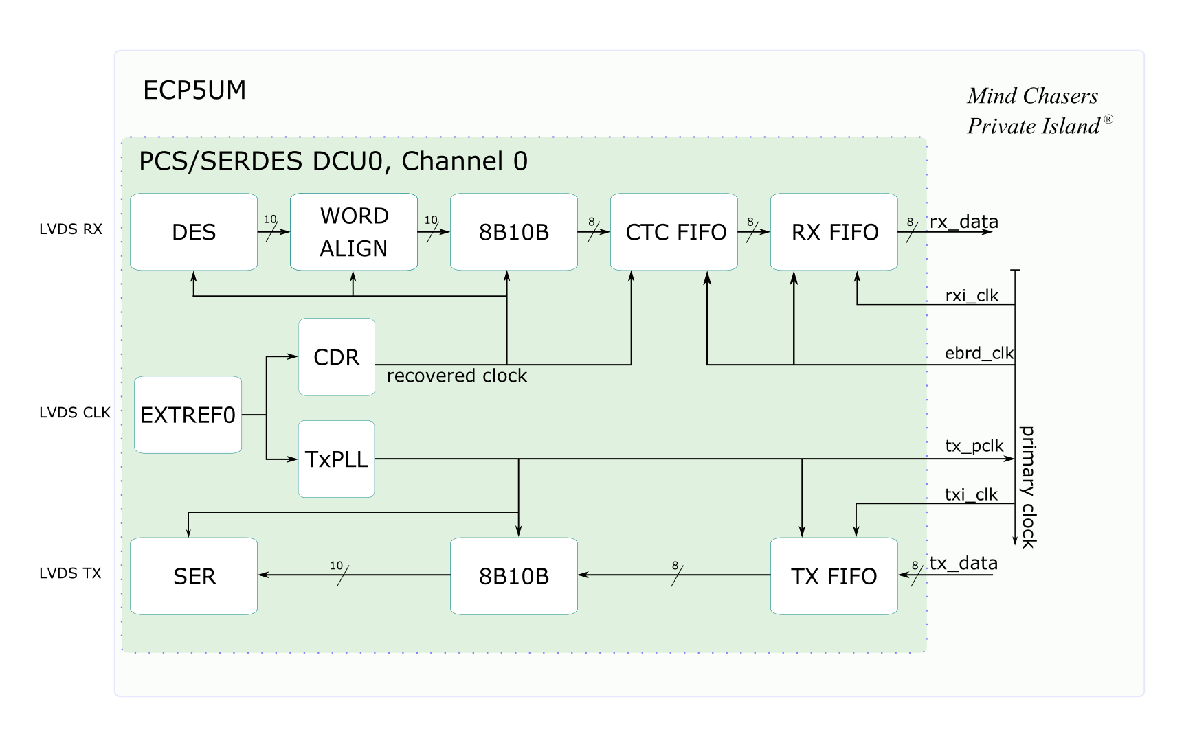
The figure below shows the clocking architecture for DCU0, channel 0, and it is similar to Figure 4 in TN1261. The output of the TxPLL is routed to the FPGA fabric as tx_pclk and used globally to clock the DCU FPGA Bridge circuits (RX FIFO, TX FIFO, and CTC FIFO) for both DCU0 and DCU1. In other words, the output of the DCU0 TXPLL is used globally to clock all Ethernet circuits in the FPGA soft logic and both DCU FPGA bridge circuits. Therefore, the other tx_pclk signals and all recovered RX CDR outputs are left floating.
SERDES/PCS Parameter
Provided below are some of the parameters that can be changed in the Clarity generated Verilog file.
RX Equalizer:
- enable: DCU1_inst.CH0_REQ_EN = "0b1";
- disable: DCU1_inst.CH0_REQ_EN = "0b0";
- equalization setting: DCU1_inst.CH0_REQ_LVL_SET = "0b10";
AC/DC coupling:
- DCU1_inst.CH0_RCV_DCC_EN = "0b0";
- DCU1_inst.CH0_RCV_DCC_EN = "0b1";
Reference Clock
- 125 MHz: DCU0_inst.D_REFCK_MODE = "0b001";
- 50 MHz: DCU0_inst.D_REFCK_MODE = "0b100";
Terms
- CTC: Clock Tolerance Compensation
- DCU: Dual Channel Unit
- FB: FPGA Bridge
- FF: FPGA Fabric
- FPGA: Field Programmable Gate Array
- PCS: Physical Coding Sublayer
- PHY: Physical Layer Device
- SB: SERDES Bridge
- SCI: SERDES Client Interface
- SERDES: Serializer (SER) / Deserializer (DES)


