
Overview
Provided below is draft documentation for the FPGA architecture and Verilog modules that comprise the Private Island ® open source project. This documentation is being updated on a regular basis. Note that the architecture portion of the documentation is generic, but implementation details are for the Betsy™ maker board.
The source code is hosted here using cgit.
Code and style conventions can be found here.
The system is highly configurable, and the developer can specify at build time various parameters including the number of PHYs to instantiate, packet filter purpose, trigger points & size, and buffer depths.
To date, the project has been deployed on Lattice ECP5UM, Lattice Certus-NX, and Altera Cyclone 10GX, 5GX, and 10LP (Betsy). The project has been customized and deployed for secure networking, video bridging, and various test & measurement applications.
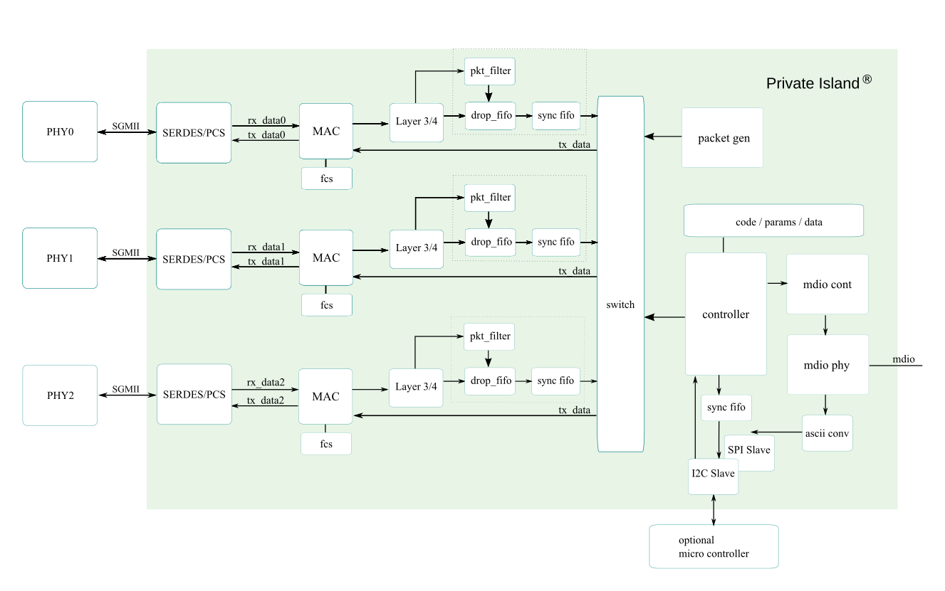
The figure below depicts an SGMII-based system with three PHYs instantiated for the purpose of connecting PHY2 to a local Linux processor. Example usage would be a network tap or a dedicated system controller port for performing higher level packet analysis, machine learning, and control. In this scenario, the system acts as an Ethernet bridge / filter / firewall between PHY0 and PHY1.
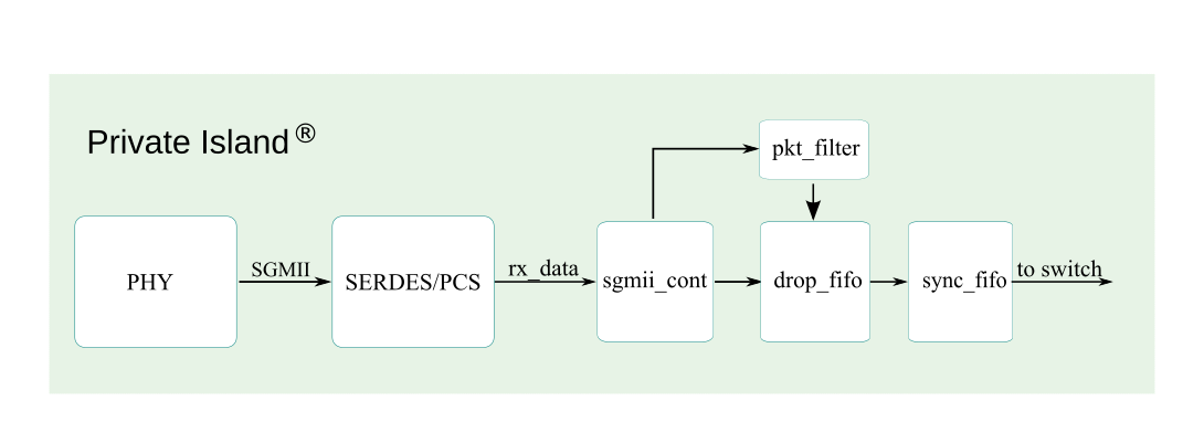
High Level Receive Path
The figure below depicts the packet data receive path. The PHY is external to the FPGA and connects via SGMII or RGMII (Betsy). The SERDES/PCS block can be a combination of vendor IP and Verilog. The remaining blocks in the figure are behavioral Verilog modules and are described further below.
TODO:
- Describe how each RX module can send data to ml engine and give reference.
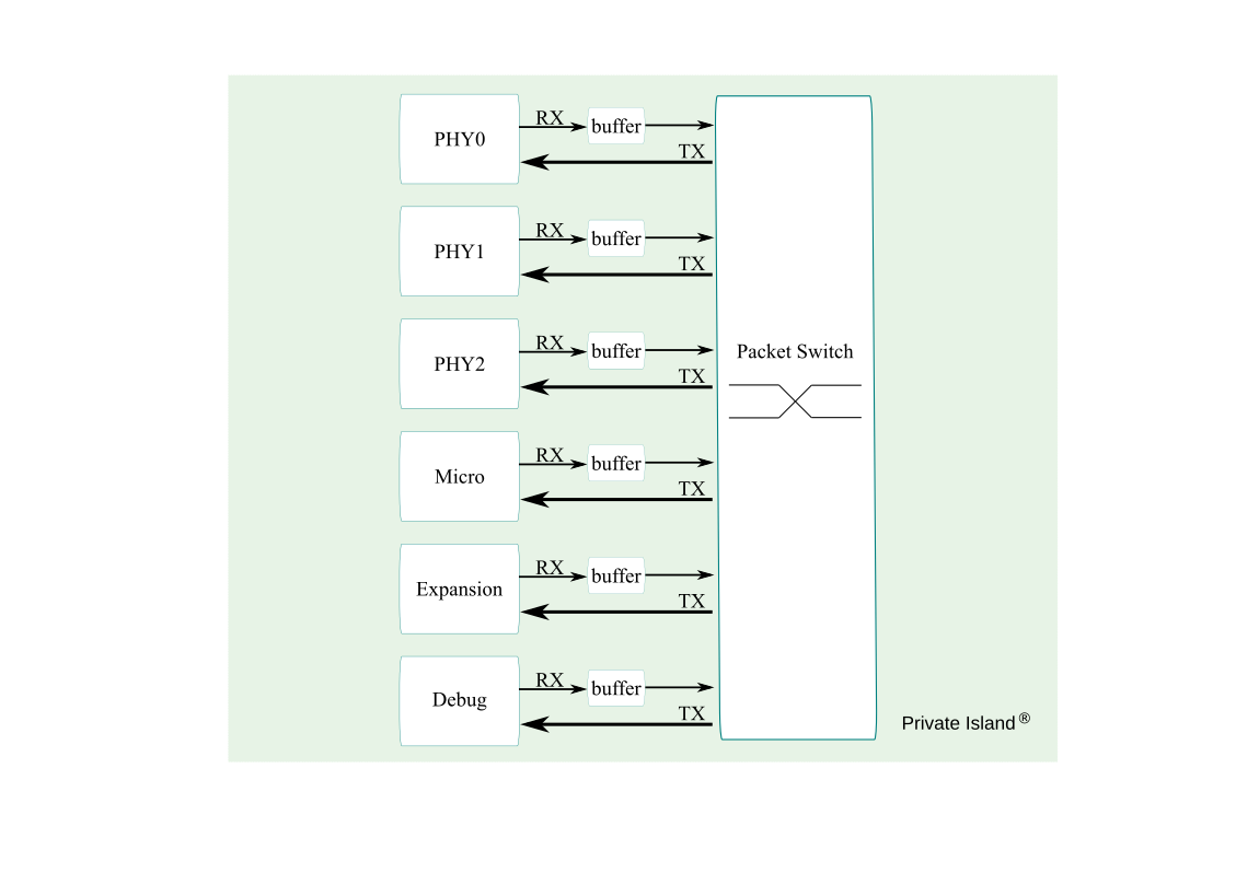
Switching
The figure below depicts the packet flow and high-level switching architecture. The packet switching is centralized and is controlled by configuring the source for each TX port.
Regardless of port, the Receive (RX) direction is into the switch, and the transmit (TX) direction is from the switch. Data buffering and filtering / dropping is typically performed in the RX direction.
Currently all 1G packet data (byte/octet wide) is clocked at 125 MHz . However, it is possible to down sample the data into a wider data path for analysis and storage functions (e.g., 32-bits @ 31.25 MHz).
Controller (controller.v)
A simplified state machine based controller is provided with the project that can receive and transmit a single 32-bit word via the LAN. This access can be used to query and modify various parameters within the FPGA implementation.
Although the controller is simplified, the implementation isn't trivial. Therefore, a separate page describing the Controller can be found here.
| Module | Address Range | Function |
|---|---|---|
| controller | 0x0000 : 0x00FF | Controller state and system params (e.g., version) |
| mac | 0x0100 : 0x01FF | MAC state information |
| pkt_filter | 0x0200 : 0x02FF | Configure each Packet Filter |
| switch | 0x0300 : 0x03FF | Configure Switch |
| mdio | 0x0400 : 0x04FF | MDIO access for each PHY |
| Address Offset | Register | Function | Size / Access / Default | Notes |
|---|---|---|---|---|
| 0x00 | fw_version | Firmware Version | 16 bits, Read Only (RO), N/A | |
| 0x04 | fw_increment | Firmware Version Increment | 16 bits, RO, N/A | Convey incremental features and bug fixes |
| 0x10 | mac_sel | MAC Selection | 8 bits, RW, 0x00 | Specify which MAC to access |
| 0x14 | mdio_sel | PHY MDIO Selection | 8 bits, RW, 0x00 | Specify which PHY to access via MDIO |
| 0x18 | pkt_filter_sel | Packet Filter Selection | 16 bits, RW, 0x0000 | Specify which Packet Filter to access |
MDIO Controller
GENERAL MAC TODO:
- why am I testing for tx_f_pkt in TX_ST_0?
- Need to enforce IPG (on TX) + look at other params in the table
- mac: why is tx_f mux combinatorial but the rest isn't?
- mac: need to review rx_pkt_length for non supported packet types. State machine should terminate early and without action.
- RX needs to detect end or start of packet and use as a reset
- Recovery, resync, don't let TX continue to run
- look at all GMII states again and map to both SGMII and RGMII
- Create an AN section below.
- AN_TX_CONFIG_LO should be 21 or 01?
mac_sgmii.v
Purpose: SGMII TX/RX/AN state machines
RX notes:
- Each frame written to the FIFO consists of the MAC destination, MAC source, Ethertype, and packet.
- Ethernet preamble and FCS are not stored
- However, the first 2 bytes of FCS are written into FIFO due to a lag issue on stopping a read during TX
- The RX packet complete bit is set on the last RX byte, so two more bytes are written after that (FCS).
- RX data written into FIFO is from rx_data_m1 register
TX notes:
- If code group /R/ is transmitted in an even-numbered position, append a single additional /R/ to the code-group stream to ensure that the subsequent /I/ is aligned on an even-numbered code-group boundary and EPD transmission is complete.
- Reading the FIFO starts two clocks early since data isn't available until after the first clock and then we register the data from the FIFO on the 2nd clock.
- Reading stops (tx_fifo_re is deasserted) after either tx_last_byte or tx_fifo_empty are detected on the next clock, These signals are expected to be coincident.
mac_rgmii.v
To be added.
| Address Offset | Register | Function | Size / Access / Default | Notes |
|---|---|---|---|---|
| 0x00 | rx_pkt_cnt | Number of RX packets | 16 bits, Read Only (RO), N/A | |
| 0x04 | tx_pkt_cnt | Number of TX packets | 16 bits, RO, N/A |
TODO:
- mac: link state
- Clean up mac_rgmii an logic
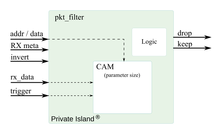
Packet Filter (pkt_filter.v and cam.v)
Purpose: packet filter / CAM wrapper with keep / drop logic
TODO:
- How to disable the CAM / pkt filtering clocking if the CAMs aren't programmed?
cam.v
Purpose: single cycle, parameterized Content Addressable Memory
Additional documentation to be added.
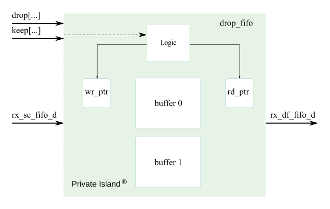
drop_fifo.v
Purpose: Double buffered side-by-side FIFO with keep / drop logic
Notes:
- Writer and Reader may either be active on first or second buffer simultaneously
- Delay (buffer depth) is set outside this module by writer ( hold off of keep or drop )
- A write can't begin on buffer[n] while a read is active on buffer[n].
- This is guaranteed to not happen as long as 2*IPG + tWR > tBuf[n]
- RX data is dropped after drop is asserted ( FIFO wr_ptr is reset ). Read on this buffer is inactive.
- FIFO buffer becomes available again after drop ( no need to switch to other buffer ).
- this lets writer drop packets early without regard to other buffer.
- FIFO is cleared on drop by setting wr_ptr to 0
- There is always a minimum gap between a need to switch buffers: FCS+IPG+PREAMBLE
- There is no empty flag since rd_ptr and wr_ptr may be pointing to different buffers.
TODO:
- Drop FIFO - drop packet if sync_fifo is almost full and not active (re-vist rules). Remember that once SF starts, it completes. Consider making sync_fifos much larger for 10G and heavy networking functions.
sync_fifo.v
Purpose: Buffer RX data until ready for TX switch
SPI
The SPI slave controller enables the external micro controller to read and write the internal memories of the FPGA.
See the following:


