
Overview
This article is a review of the power circuits on the Arduino Uno Rev3 and Mega 2560 Rev3. We're designing shields for both of these boards, so in addition to reading Arduino's user documentation, it's important for us to reverse engineer, understand, and document the capabilities and limitations of the power circuits and related connector I/O.
The on-board power circuits are simple, low cost, and rely on Low Drop Out (LDO) linear regulators for power conversion. Also, it appears that the power circuits for UNO and MEGA are virtually identical.
For the purpose of our analysis, we have downloaded the UNO and MEGA design files from the Arduino website (see references below) and imported them into Altium Designer. We also have an UNO and MEGA on our lab bench with a programable power supply & scope. The circuit pack snippets shown in the figures below are taken from screen shots of the design files within Altium Designer.
Disclaimer: Our notes below are based on an informal study & review. We are not the designer of these boards, and the information provided below may be inaccurate. Also, use caution when working with low voltage power circuitry as improper use may cause smoke, fire and / or skin burns.
The notes below should be read along with Arduino's online power documentation.
Stack up and Ground
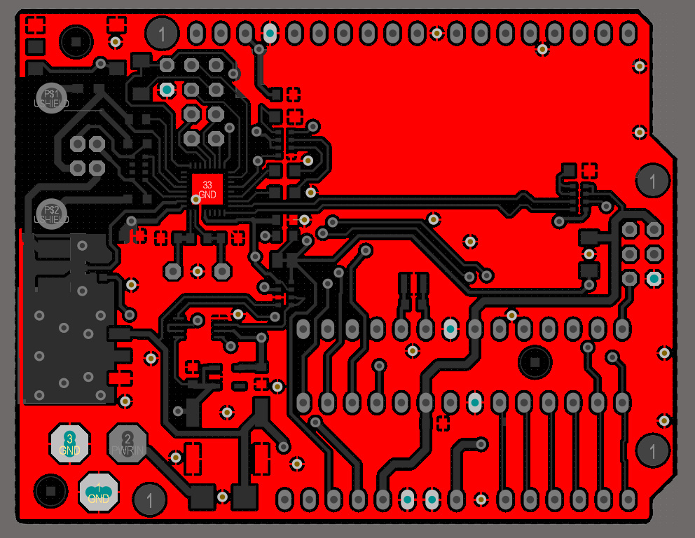
Both UNO and MEGA are two layer boards. There are no internal power or ground planes. Instead, copper ground pours have been liberally placed around the routing of signals and power traces (see figure below, ground is shown in red). The use of a two-layer board is consistent with low cost; however, the lack of a ground plane will lead to circuit loops and inconsistent characteristic impedance / signal reflections. This can make for a noisy board from the view of electromagnetic radiation, especially when the frequencies and currents increase.
Also note in the figure below the lack of ground pins on the peripheral I/O connectors. This creates signal integrity challenges when designing a shield for an UNO (or MEGA) base.
Power Rails
Arduino UNO and MEGA rely on LDO linear regulators for power conversion (e.g., 5V to 3.3V). If you're not familiar with a linear regulator, you can still move forward at this point by conceptualizing that it works like an adaptive resistor that provides a constant voltage to a load under varying current conditions. This adaptive resistance is provided by a transistor within the regulator, and the term "drop out" refers to the condition when the transistor / regulator can no longer regulate the voltage. Drop out occurs when the difference between the input and output voltages fall below a minimum threshold.
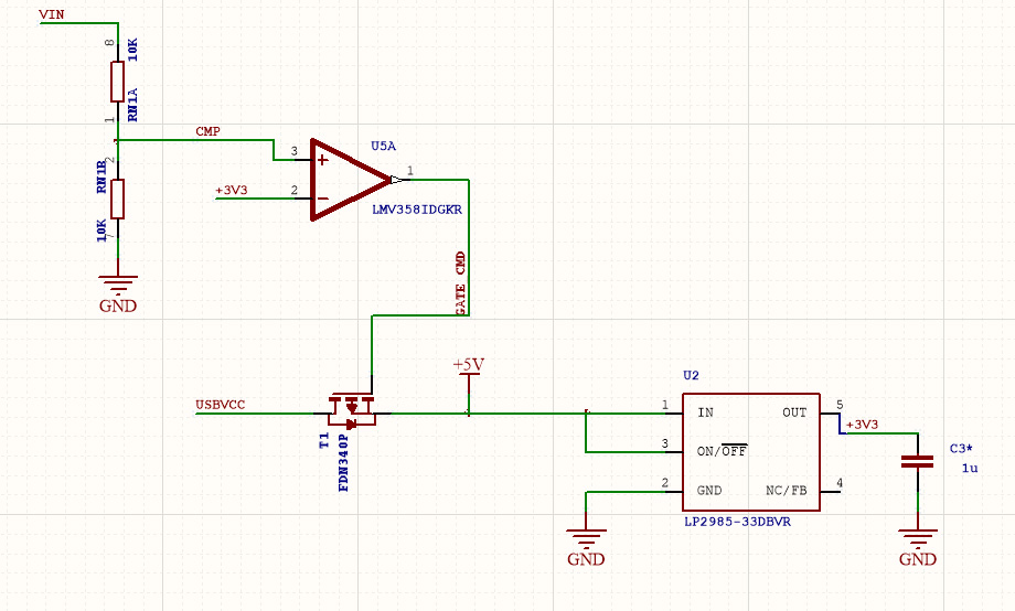
As you probably already know, UNO and MEGA can be powered via either the USB jack or the barrel connector (see figures 2 and 3 below). If both voltage supplies are supplied simultaneously, the voltage on the barrel connector wins out as long as its slightly greater than twice 3.3V (our tests showed ~7.2V). At this voltage, the op amp in Figure 3 (U5A) drives high and turns off the P-channel FET (T1). Remember that P-channel FETs turn on when the gate voltage is low (GATE_CMD signal).
Note that Arduino states 7V is within its recommended range for VIN. Our testing shows that VIN near 7V can lead to a situation where the system switches back and forth between being powered by USB and the barrel jack (VIN), depending on load and its regulation. We suspect the use of VIN @ 7V could create an unstable system and should be avoided. Also, when working with Arduino with USB and a VIN power supply below 8V, it is a good idea to monitor the FET's GATE_CMD signal to confirm that it is stable.
As Figure 2 shows, the barrel jack voltage supply, which must be greater than 5V, is supplied to a 1.0 A OnSemi NCP1117 LDO fixed-volgate regulator. This is an extremely simple circuit, but keep in mind that it is very inefficient, especially when using a 12V wall wart (efficiency ~= 5/12 = 40%). If you're drawing near 1A, the power loss will be near 7W! Also, note that this input does not appear to be fused.
Arduino tells it's users not to supply 5V on the 5V I/O connector, and the circuit in Figure 2 shows that driving 5V directly means driving the output of the LDO, and this is typically a bad idea. Figure 3 conveys the same concept for 3.3V (don't back drive the output of a regulator).
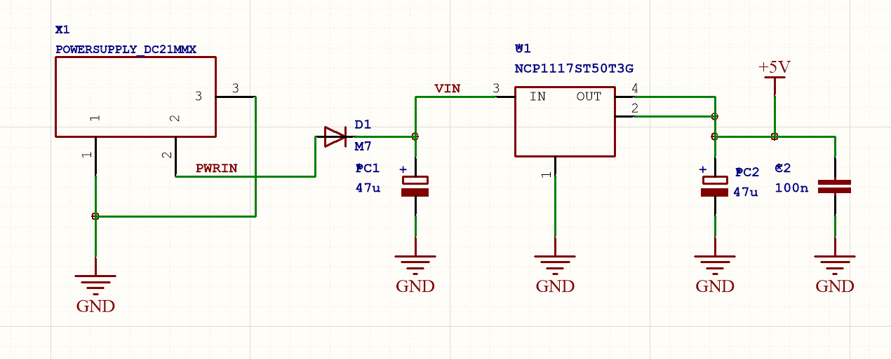
Figure 3 shows how the aforementioned P-channel FET (T1) is used to either switch the USBVCC onto the 5V rail or isolate it, depending on the value of VIN (barrel jack supply). Either way, the 5V rail feeds into a Texas Instruments 150 mA 3.3V LP2985 LDO. Arduino recommends not drawing more than 50 mA1 even though the regulator appears to be rated higher. We suspect this is due to managing the overall power / current on the board when using a USB supply, which is limited to 500 mA. Also, heat / power dissipation may be an issue.
Regarding power dissipation and heat, this can be a substantial issue when using a shield and drawing a lot of current from the regulators. In these instances, it's probably a good idea to use inter-board connectors with long posts.
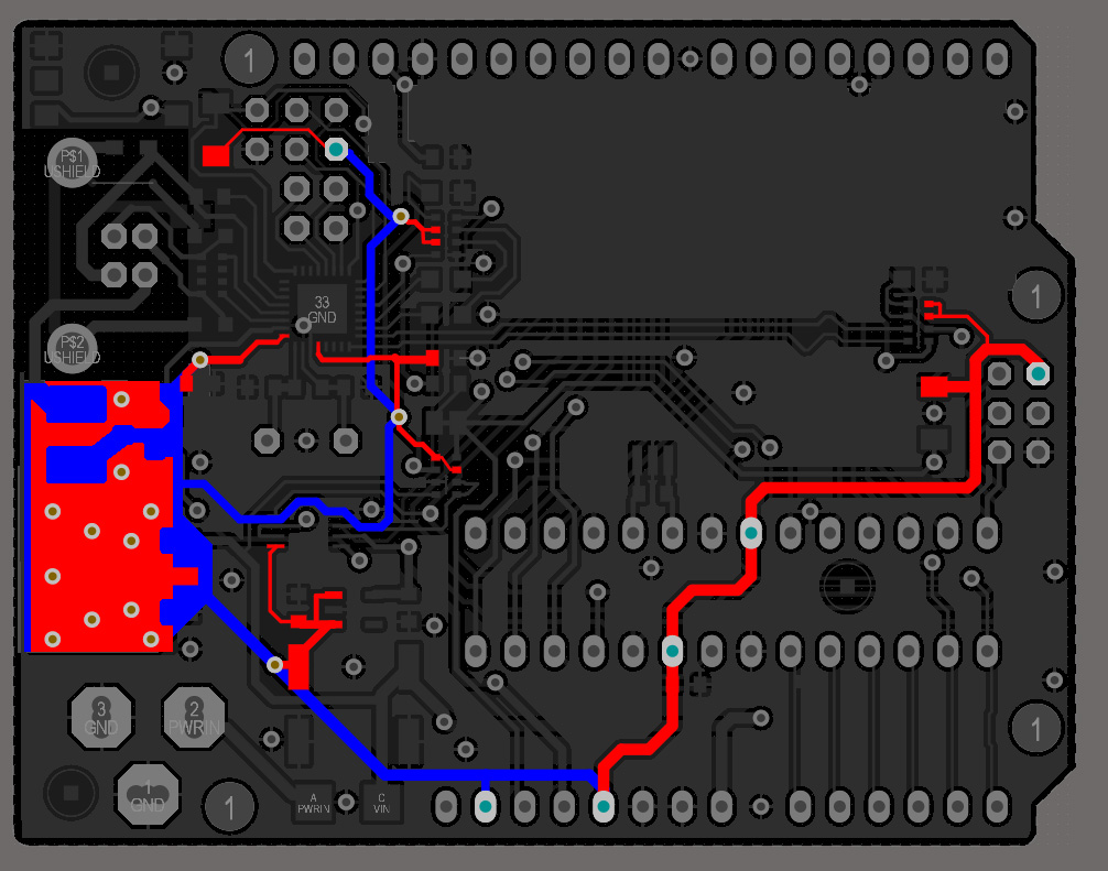
PCB Screen Shots
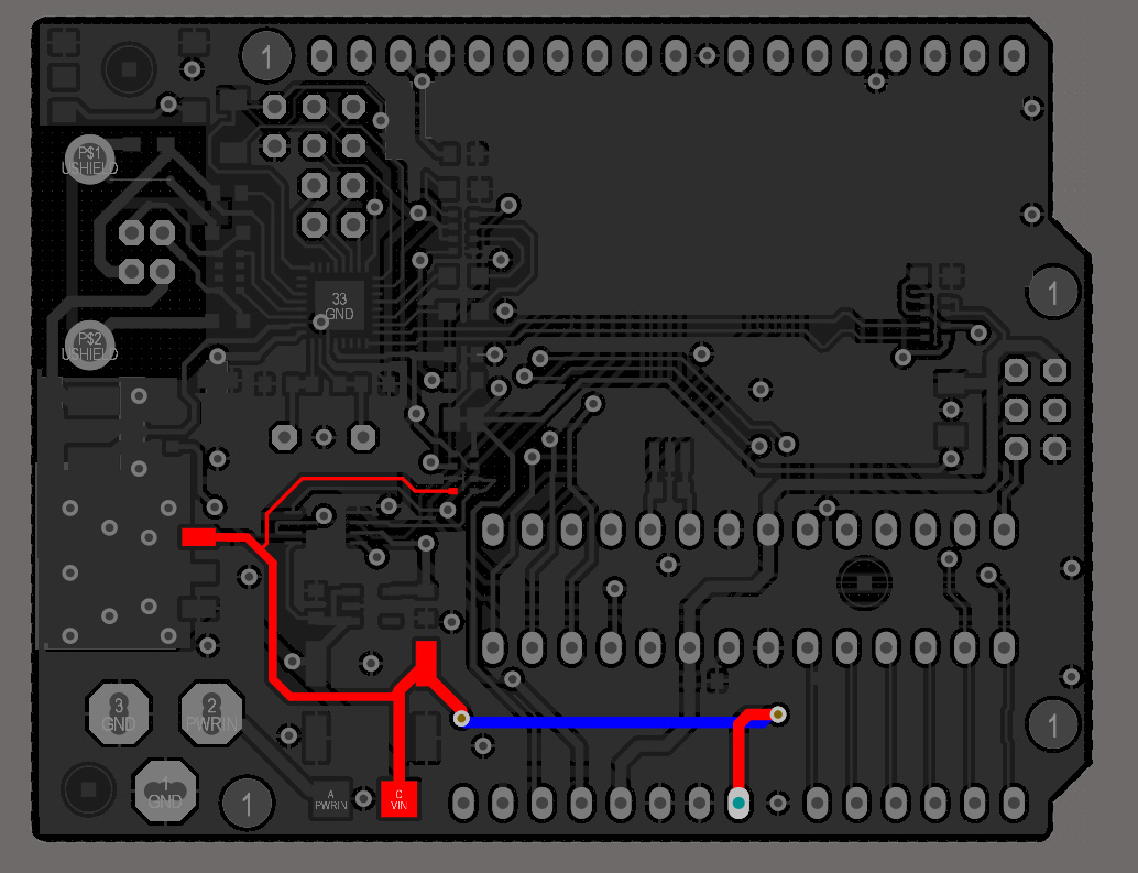
Figures 4 and 5 below show the routing of VIN and +5V respectively. Red is the top of the board, and blue is the bottom of the board. Note in Figure 5 that IOREF is tied directly to 5V.
Summary
We'll continue to update this article as we develop & improve our shields for the Arduino ecosystem.
Our analysis has shown us the following regarding shield design:
- A shield with on-board, high efficiency switching regulators should power the base via VIN. This will save considerable power and heat.
- If the shield powers the base, leave the 3V and 5V pins disconnected.
Please let us know below if we have mis-stated something or you want us to add certain information.
References and Footnotes
- We're told by a member on Reddit that the 3.3V 50mA recommendation is a holdover from previous designs that relied on an FTDI device for 3V regulation.


