Overview
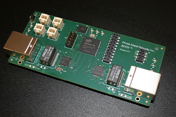
The Betsy v0.1 board shown in the figure below is the initial prototype for the FPGA-based maker board. This board is currently being used for the first phase of beta trial to solicit feedback and develop & debug the initial implementation of the Private Island ® open source project customized for Betsy.
As shown in the block diagram below, Betsy is powered by the low cost, general purpose Altera Cyclone 10 LP. This FPGA device is an excellent choice for a networking maker board since its I/O can support a Gigabit RGMII interface. This eliminates the need to use encrypted IP modules for the network interface, such as PCS / SERDES. This provides the ultimate in transparency and flexibility for an FPGA-based design.
Note that questions regarding the Cyclone 10 LP can be posted on our forum or the Altera forum.
An overview of the Cyclone 10 LP used on Betsy is listed below:
- 10CL025YU256
- 25K Logic Elements
- 66 9K memory blocks
- 132 9x9 multipliers
- 4 PLLs, 20 Global Clocks
- 60 nm process
- Core voltage: 1.2V
- UBGA package, 256 balls (14 mm x 14 mm, 0.8 mm pitch)
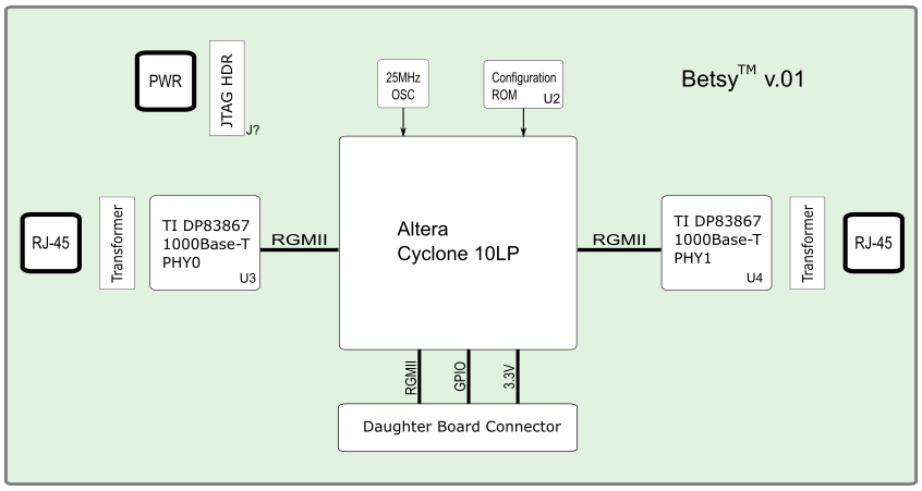
Cyclone 10 LP Bank Assignments:
| Bank(s) | Schematic Sheet | Notes |
|---|---|---|
| Bank 1 | Configuration | ROM and JTAG |
| Banks 2, 3 | RGMII0 | Routed to PHY0 |
| Banks 4, 5 | RGMII1 | Routed to PHY1 |
| Banks 6, 7 | RGMII2 | Routed to Daughter Board Connectors |
| Bank 8 | Expansion | Clock, LEDs, Reset, and Daughter Board Connectors |
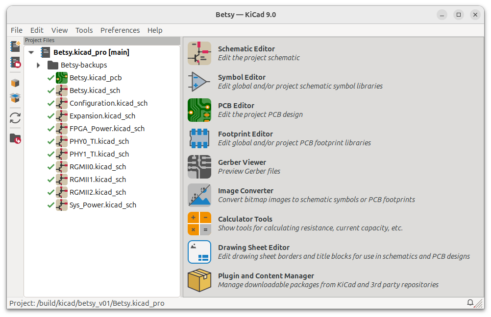
Betsy Hardware Design, Kicad Import
A KiCad import of both the schematic and PCB design are hosted on our site here. A description of each schematic sheet is provided below.
Before reviewing the text below, you should first clone the betsy_v01 repo and open the project in KiCad 9.0. After opening the project, your view of the (imported) project should be similar to what is shown in the screenshot below.
Please make sure to review the README.txt file included in the project folder for important project information.
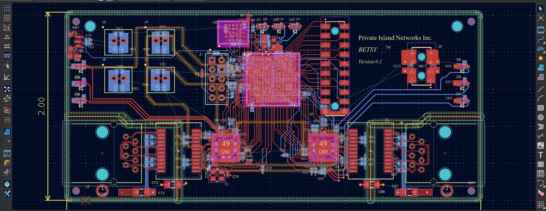
Shown below is a view of the Betsy PCB in the KiCad PCB editor. Keep in mind that this is an import and may contain problems that were caused by the import process from Altium.
Schematic Description
The schematic sheets are described below in the order shown in the KiCad project screenshot above.
Betsy.kicad_sch
This is the top level sheet that instantiates the nine design sheets.
Note that the wrong FPGA bank may appear when a schematic sheet is opened directly. If you experience this, then open each sheet from the top sheet.
Configuration.kicad_sch
The configuration ROM is a Micron 128 Mbit, 3.3V MT25QL128 device. Additional I/O is routed between the device and the FPGA to support the octal MT35X Xccela device. This optional high-speed, DDR capable ROM is supported with machine learning applications in mind.
A 10-pin header is provided for JTAG (programming and debugging) support.
The next revision of Betsy will most likely support an onboard FTDI device to eliminate the need for an external JTAG programming adapter. For more information on this topic please see Use an FTDI Mini Module as an Altera USB Blaster III Programming Adapter
Expansion.kicad_sch
Two Samtec HLE surface mount connectors are provided to support Betsy daughter boards. A Gigabit Ethernet daughter board already exists and more are planned. Examples of boards planned are a GPIO break out board and a machine learning Inferencing Engine.
The HLE I/O routing defines a third RGMII interface. However, this I/O can be redefined to support other daughter board applications.
A 25MHz Abracon clock oscillator is provided as a general purpose clock.
A TE reset switch is provided to perform a full asynchronous reset of the FPGA device. This can be redefined for other applications if desired.
Three general purpose LEDs (0:2) are provided.
FPGA_Power.kicad_sch
This sheet shows the FPGA power connections for the 1.2V core voltage and 2.5V auxillary voltage.
The I/O bank voltages are shown on the other sheets where each FPGA bank is instantiated.
PHY0_TI.kicad_sch and PHY1_TI.kicad_sch
The Gigabit Ethernet PHY used for Betsy is the Texas Instruments (TI) DP83867CS.
The schematic sheets for the TI PHY are identical with the exception of the crystal driving PHY0. This is used to create a low jitter 25MHz clock that is input to the FPGA. This can be used to generate other PHY clocks in the system.
Note that questions regarding the DP83867CS can be posted on our forum or on the TI forum.
The TE 5558342-1 RJ45 jack does not provide integrated LEDs. Therefore, each PHY circuit provides three discrete PHYs, which are driven directly from the PHY. The definition of each LED can be modified via registers internal to the PHY. These are configured via the PHY MDIO interface.
RGMII0.kicad_sch through RGMII2.kicad_sch
The three RGMII related schematic sheets are basically I/O routed to different FPGA banks. The selection of each bank is driven mainly based on the location of the bank I/O relative to the PHYs and expansion connectors.
Note that the RGMII specification specifies a tight timing relationship for the bus and clock, and this requires careful consideration to minimize and control routing lengths.
Sys_Power.kicad_sch
System power for the initial prototype is provided via connectors to an external source. Supported sources are external lab bench type supplies and small, custom, integrated power modules, which are typically provided with each Betsy board.
The next revision of Betsy will have integrated power and require only a single low-power source, such as 5V or 12V.


